The chemical etching process forms pyramidal textures or inverted pyramid structures on silicon wafer surfaces, significantly enhancing light absorption efficiency in photovoltaic cells. This critical manufacturing process is essential for improving solar cell conversion efficiency.

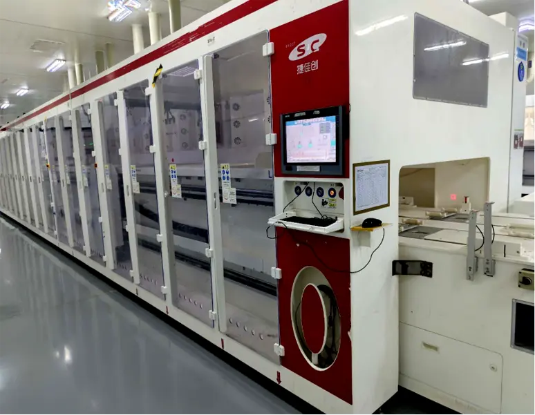
Equipment : Monocrystalline batch texturing system
Manufacturer Choice: CHINA S.C.,Kingenious.,etc
P+ Layer Formation for PN Junction: Using BCl₃ at high temperatures to form a P+ layer on the silicon wafer surface, thereby creating a PN junction that enables carrier generation in the wafer.
N-type Cell Junction Formation Method: The junction formation process for N-type cells involves diffusing boron (B) into phosphorus-doped semiconductor material, creating a P-N junction at the interface between the two doped semiconductor regions.
Equipment :
Boron diffusion furnace(6 tube)
Manufacturer Choice:
CHINA S.C.,Laplace.,etc
Phosphosilicate Glass (PSG) Removal Using HF
Reaction: SiO2+HF-H2SiF6+H2O
Selective Surface Passivation & Polishing Mechanism:
“Protective groups” (e.g., silane-based compounds) form an ordered monolayer on the oxide surface:
Creates OH⁻ diffusion barrier → Prevents SiO₂ etching
Accelerates OH⁻ reaction with backside Si → Enhances anisotropic etching on {111}/{100} planes
Equipment: In-line BSG removal equipment+Alkali polishing equipment
Manufacturer choice: CHINA S.C.,Kingenious.,etc
Oxide Layer Deposition Principle: Thermal oxidation via oxygen diffusion at elevated temperatures, where oxygen reacts with silicon to form silicon oxide.
Chemical Reaction: O2+SiSiOx。
Amorphous Silicon (a-Si) Deposition Principle: Thermal decomposition of silane (SiH₄) in CVD process, producing solid-phase silicon and hydrogen byproducts.
Chemical Reaction: SiH₄(g) → Si(s) + 2H₂(g)
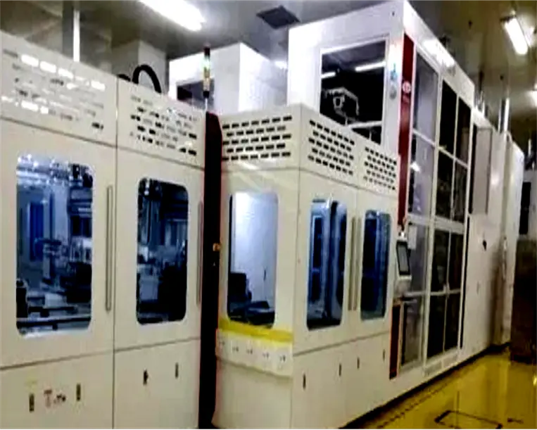
Equipment: LPCVD system
Manufacturer choice: Laplace.,etc
The P2O5 produced by the decomposition of POCl3 is deposited on the surface of the silicon wafer. P2O5 reacts with silicon to generate SiO2 and phosphorus atoms, and forms a layer of phosphosilicate glass on the surface of the silicon wafer. The phosphorus atoms then diffuse into the silicon.
Reaction: 2P2O5+5Si=5SiO2+4P↓
Equipment: Phosphorus diffusion furnace
Manufacturer choice: CHINA S.C..,etc
Inline Wet Etching for PSG Removal (Back & Sidewalls)
Process: Chain-type wet station uses HF-based chemistry to remove phosphosilicate glass (PSG) from wafer backside and edges before RCA cleaning.
The “protective groups” are selectively arranged in an orderly manner to enhance the protection of BPSG. After removing PSG on the POLY surface using an alkali polishing process, aOH+ADD is used to successfully protect SiO2 from being corroded by NaOH.
Equipment: In-line PSG removal system+RCA cleaning machine
Manufacturer choice: CHINA S.C..,etc
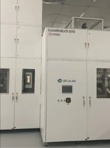
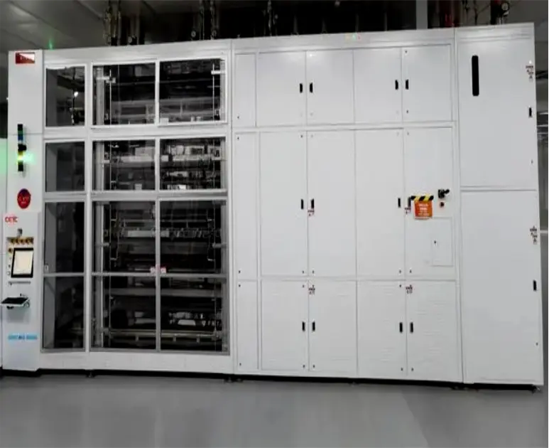
Surface Passivation Principle: ALD enables layer-by-layer deposition of atomic-scale thin films. Using Al₂O₃’s negative fixed charges, it creates an interface electric field directed toward the silicon bulk. This field:
Repels electrons from the Al₂O₃/Si interface in n-type silicon
Reduces interface recombination velocity (Seff < 10 cm/s)
Enhances minority carrier lifetime (Δτ > 1 ms)
Al₂O₃ Deposition via TMA Precursor Reaction Mechanism: Trimethylaluminum (TMA) reacts with water vapor in a cyclic process:
2AL(CH3)3 + 3H2O = Al2O3 + 6CH4
Equipment: ALD
Manufacturer choice: LEADMICRO.,etc
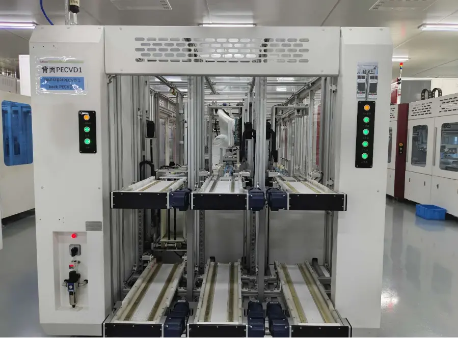
Low-temperature plasma serves as the energy source, with the silicon wafer placed on the cathode under low-pressure glow discharge. The wafer is heated to a predetermined temperature through glow discharge (or an additional heating element). An appropriate amount of SiH₄ and NH₃ is then introduced, undergoing a series of chemical and plasma reactions to form a solid thin film (SiNₓ) on the front surface of the silicon wafer.
Equipment: 5-tube front-side plasma-enhanced CVD
Manufacturer choice: CHINA S.C..,etc
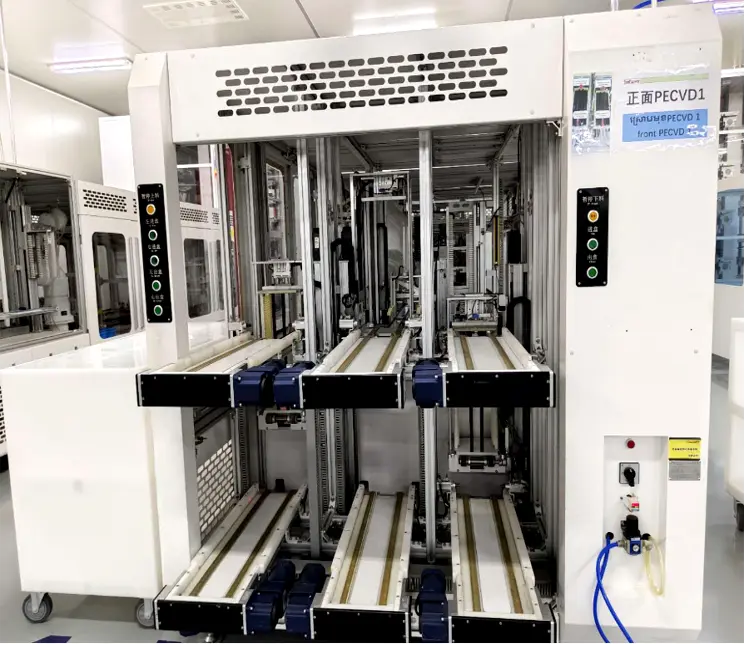
Using low-temperature plasma as the energy source, the silicon wafer is placed on the cathode of a low-pressure glow discharge system. The wafer is heated to a predetermined temperature through glow discharge (or with an additional heating element). An appropriate amount of SiH₄ and NH₃ is then introduced, undergoing a series of chemical and plasma reactions to form a solid thin film (SiNₓ) on the back surface of the silicon wafer.
Equipment: 5-tube back-side plasma-enhanced CVD
Manufacturer choice: CHINA S.C..,etc
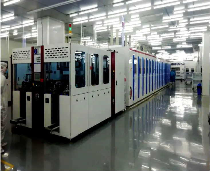
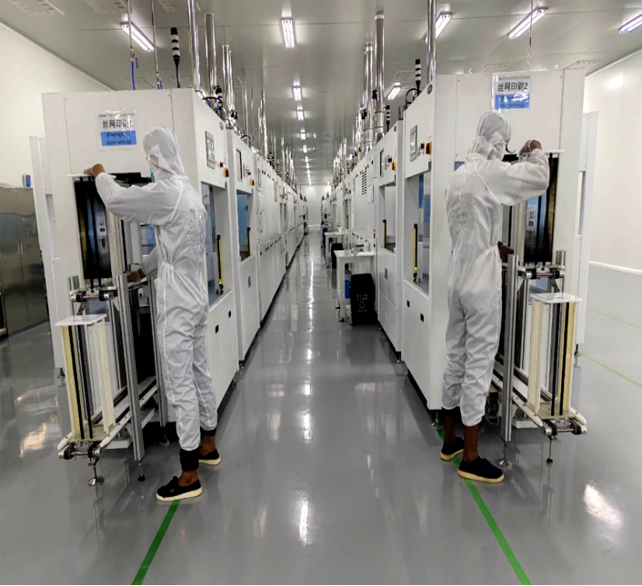
During printing, paste is applied onto the screen mesh. The squeegee exerts controlled pressure while traversing the screen, forcing the paste through the mesh openings onto the substrate. The paste adheres within defined boundaries due to its viscosity.
A controlled gap between screen and substrate enables the tensioned screen to rebound from the squeegee, maintaining only a moving line contact. This creates paste-snap-off from the mesh during separation, ensuring dimensional accuracy. Post-printing, the squeezee lifts and the screen retracts, while a flood bar returns excess paste to the starting position – completing one print cycle.
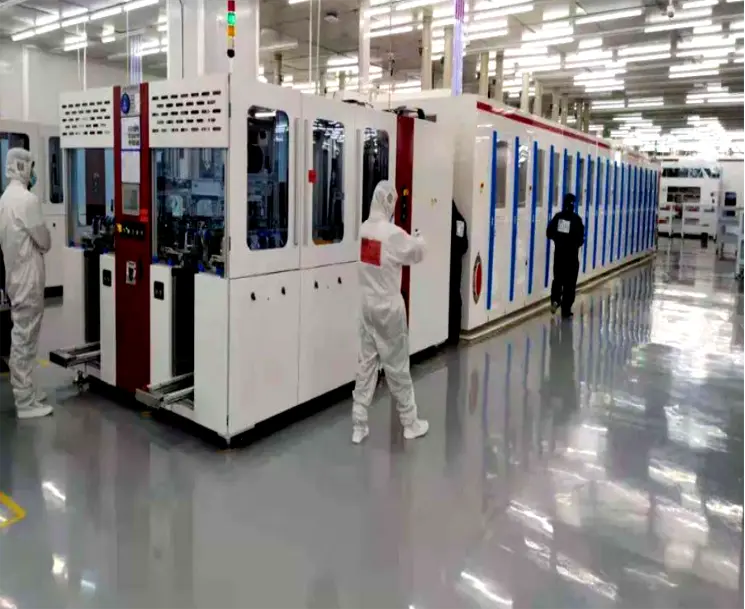
Equipment: Dual-track screen printing line
Manufacturer choice: CHINAMAXWELL.,etc
Low-Temperature Zone: Primarily involves the evaporation and combustion of the paste’s organic solvents and binders.
Intermediate-Temperature Stage: Mainly characterized by the melting of the glass frit and the aggregation of silver particles.
High-Temperature Stage: Dominated by reactions between silver, silicon, and molten glass, forming silver-silicon alloys.
Cooling Phase: Primarily consists of the recrystallization and grain growth of silver particles on the silicon surface.
Equipment: Firing furnace & light injection integrated system(Dual-track)
Manufacturer choice: CHINAMAXWELL.,etc
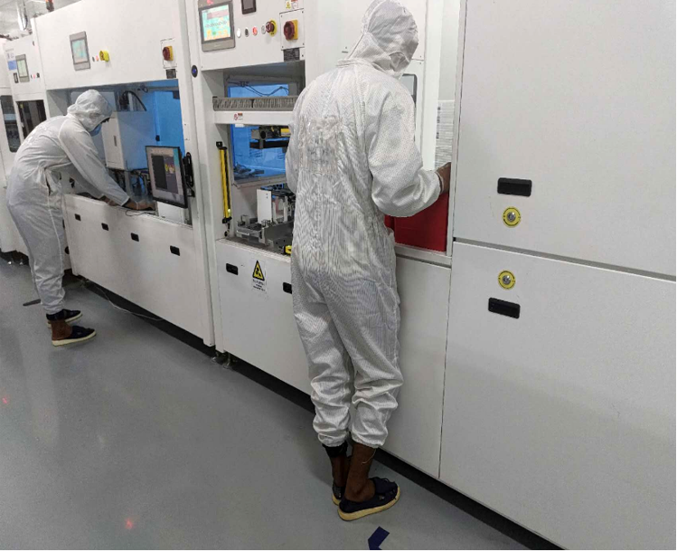
High-intensity laser irradiation excites charge carriers in the solar cell, while a bias voltage exceeding 10V is applied, generating a localized current of several amperes. This induces sintering, triggering mutual diffusion between the silver paste and silicon, significantly reducing the contact resistance between the metal and semiconductor, thereby improving the fill factor. Meanwhile, throughout the sintering process, the carrier lifetime rapidly terminates after the laser passes, minimizing damage to the original passivation layer.
Equipment: Dual-track laser-induced doping system
Manufacturer choice: DR.,etc
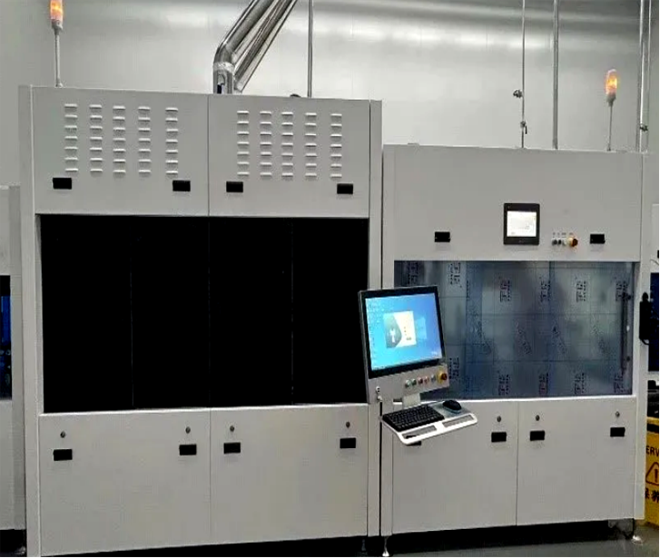
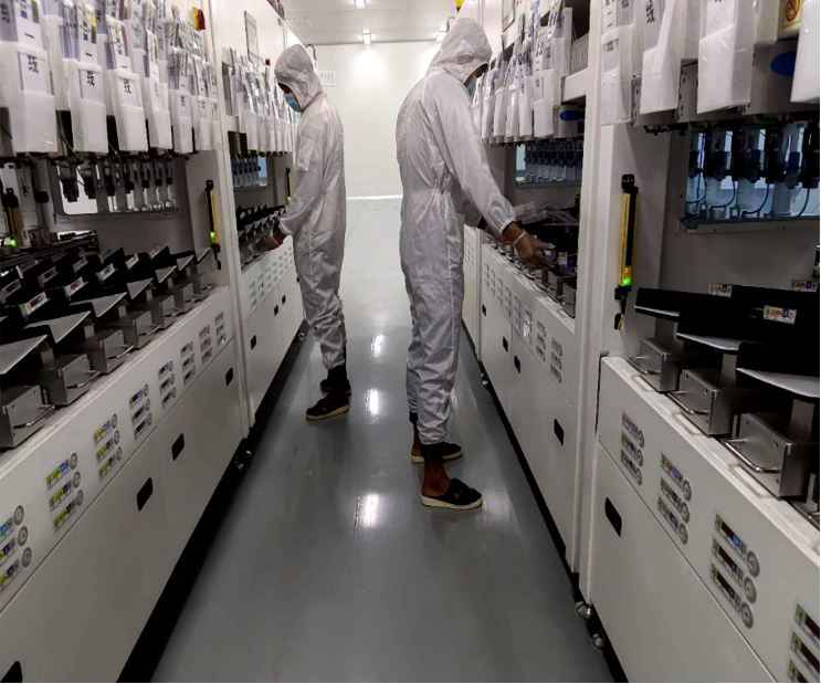
AOI (Automated Optical Inspection) is a device based on optical principles to detect common visual defects encountered during solar cell production.
EL (Electroluminescence) Principle: A forward current is applied to the solar cell, utilizing the inverse process of the photovoltaic effect to make the cell emit light. The imaging system captures the signal and transmits it to computer software, which processes the data and displays the EL image of the solar cell on the screen.
IV Tester Principle: The solar cell is exposed to simulated sunlight, converting light energy into electrical energy and generating current. The tester simultaneously measures current and voltage, then calculates key parameters such as power and efficiency based on the data.
Equipment: Dual-track solar cell tester & sorter (HALM system, 150-bin)
Manufacturer choice: CHINAMAXWELL.,etc
To find out more about our products and solutions, please fll out the form below and one of our experts will get back to you shortly
3000 TPD Gold Flotation Project in Shandong Province
2500TPD Lithium Ore Flotation in Sichuan
Fax: (+86) 021-60870195
Address: No.2555,Xiupu Road, Pudong, Shanghai
Copyright © 2023. Prominer (Shanghai) Mining Technology Co.,Ltd.


